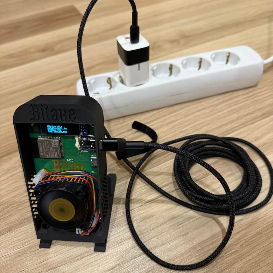
Conversion to 12V input for Bitaxe Gamma

Rationale for increasing Input Voltage:
1. To address the limitations of rare and specialized power supplies, it is recommended to adopt a standardized power supply range. The current 5V 6A configuration is impractical, especially when using a DC jack, as high current levels can cause contact resistance issues. Transitioning to a 12V power supply offers a more efficient solution. For the same 30W power output, a 12V 2.5A supply is sufficient, reducing voltage drops in conductors and contacts by over 58%.
2. During self-tests using a 5V 6A Mean Well power supply voltage drops were recorded on capacitors 5V0 -> C2; 1V2 -> C43:

3. Adopting a 12V input is essential for future development objectives, such as USB-C PD implementation and PCIe slot miner development:
- USB-C PD: The maximum current available at 5V is limited to 3A, necessitating an increase in input voltage to 12V or 15V to meet power requirements via USB-C PD.
- PCIe Slot Compatibility: PCIe slots provide only 12V and 3.3V voltages, making a 12V input indispensable for miner device functionality.
Hardware implementation process:
1. Replace all relevant capacitors with higher voltage rating ones.C2; C3; C4; C6; C7; C9; C5; C51; C52 -> change to 16V-25
Some replacements may exceed the original footprint size but can be soldered with appropriate adjustments.
Some replacements may exceed the original footprint size but can be soldered with appropriate adjustments.
2. Convert whole 5V bus to 12V bus. Disconnect U5 and U6 from 5V (12V) rail. Remove U3:

3. Add switch mode converter to 12V rail and set output voltage to 3.3V, so 3.3V rail is created.

4. Connect U4, U5, U6 to 3.3V rail.

5. U2 is sensing voltage (feedback) noticeably far away from the load. By using currents up to 20A, is very important to connect sensing conductors as close as possible to load. Especially if there are vias in the current way.


To eliminate possibly wrong feedback measurements straight twisted sensing line was made and connected to C39.

By simulating TPS546D24 design with WEBENCH Power Designer, was noticed that input and output capacitance is not sufficient. Designer shows quantity of capacitors, so it can be confusing. So extra capacitance was added (but also it was under recommended values due to lack of space).


Software implementation process:
Since FW is designed to work with hardware which supports only 5V nominal input voltage. Slight changes for code constants is needed.
Modification was made to TPS546.h header file:

Testing:
Post-modification testing demonstrated comparable performance to the original 5V configuration. However, U2 exhibited slightly elevated temperatures due to a larger voltage drop in the internal LDO. This can be mitigated by integrating an external 5V switching regulator to bias the internal LDO, enhancing efficiency.


Next steps:
1. Incorporate USB-C PD compatibility to support power banks and compact phone chargers.2. Design a new PCB to optimize thermal and energy performance, facilitating accurate testing and eliminating the complexities of wire-fixed prototypes. Since wire-fixed prototype testing is a bit tricky, you never know are you testing device or wire-fixes.
3. Perform comparative testing with the 12V prototype to validate improvements.
